Accessibility Statement Skip Navigation
  • Back to Global Sites
  • +972-77-2005042
  • Blog
  • Journalists
  • GDPR
  • Send a Release
PR Newswire: news distribution, targeting and monitoring
  • News
  • Products
  • Contact
Search
When typing in this field, a list of search results will appear and be automatically updated as you type.

Searching for your content...

No results found. Please change your search terms and try again.
  • News Releases view all

    • Hamburger menu
    • PR Newswire: news distribution, targeting and monitoring
    • Send a Release
      • Telephone

      • +972-77-2005042 from 8 AM - 11 PM IL

      • Contact
      • Contact

        +972-77-2005042
        from 8 AM - 11 PM IL

    • Searching for your content...

      No results found. Please change your search terms and try again.

      News Releases

      view all
      Close menu
    • News
    • Products
    • Contact
      • Request More Information
      • Journalists
      • GDPR

      NEO Semiconductor Introduces World's First Extreme High Bandwidth Memory (X-HBM) Architecture for AI Chips

      NEO Semiconductor Logo (PRNewsfoto/NEO Semiconductor)

      News provided by

      NEO Semiconductor

      05 Aug, 2025, 16:00 IDT

      Share this article

      Share this article


      New X-HBM architecture delivers a 32K-bit wide data bus and potentially 512 Gbit per die density, offering 16X more bandwidth or 10X higher density than traditional HBM

      SAN JOSE, Calif., Aug. 5, 2025 /PRNewswire/ -- NEO Semiconductor, a leading developer of breakthrough memory technologies, today introduced the world's first Extreme High Bandwidth Memory (X-HBM) architecture for AI chips. Built to meet the growing demands of generative AI and high-performance computing, X-HBM delivers unmatched performance with a 32K-bit data bus and potentially 512 Gbit per die, dramatically surpassing the limitations of traditional HBM with 16X greater bandwidth or 10X higher density.
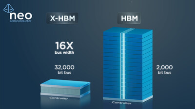
      NEO Semiconductor unveils X-HBM™ architecture, the world’s first Extreme High Bandwidth Memory for AI chips—offering 16X more bandwidth or 10X higher density than traditional HBM, enabling faster, more energy efficient, and scalable AI performance
      NEO Semiconductor unveils X-HBM™ architecture, the world’s first Extreme High Bandwidth Memory for AI chips—offering 16X more bandwidth or 10X higher density than traditional HBM, enabling faster, more energy efficient, and scalable AI performance

      "X-HBM is not an incremental upgrade, it's a fundamental breakthrough," said Andy Hsu, Founder & CEO of NEO Semiconductor. "With 16X the bandwidth or 10X the density of current memory technologies, X-HBM gives AI chipmakers a clear path to deliver next-generation performance years ahead of the existing roadmap. It's a game-changer for accelerating AI infrastructure, reducing energy consumption, and scaling AI capabilities across industries."

      Built on NEO's proprietary 3D X-DRAM architecture, X-HBM represents a major leap in memory technology by eliminating long-standing limitations in bandwidth and density. In contrast, HBM5, still in development and expected to reach the market around 2030, is projected to support only 4K-bit data buses and 40 Gbit per die. A recent study from the Korea Advanced Institute of Science and Technology (KAIST) projects that even HBM8, expected around 2040, will offer just 16K-bit buses and 80 Gbit per die. In comparison, X-HBM delivers 32K-bit buses and 512 Gbit per die, allowing AI chip designers to bypass a full decade of incremental performance bottlenecks associated with traditional HBM technology.

      Key Features and Benefits:

      • Scalable – Enables faster data transfer between GPUs and memory for more efficient AI scaling.
      • High-Performance – Unlocks untapped GPU capabilities to boost AI workloads.
      • Sustainable – Reduces power and hardware needs by consolidating AI infrastructure.

      NEO Semiconductor's CEO, Andy Hsu, will deliver a keynote presentation on August 6, at 11 a.m. PST at FMS: the Future of Memory and Storage, where he will discuss the breakthrough X-HBM technology. The event takes place August 5-7, 2025, at the Santa Clara Convention Center in California, USA. NEO Semiconductor will also be exhibiting at booth #507. To schedule a meeting at FMS 2025, please contact: [email protected].

      About NEO Semiconductor
      NEO Semiconductor is a high-tech company pioneering next-generation memory technologies, including 3D NAND flash, 3D DRAM, and 3D AI solutions. Founded in 2012 by Andy Hsu in San Jose, California, the company holds over 30 U.S. patents. NEO's key innovations include X-NAND™, which delivers SLC performance from TLC and QLC memory, and X-DRAM™, the world's lowest-power DRAM architecture. In 2023, NEO introduced 3D X-DRAM™, the first DRAM built on a 3D NAND-like structure to overcome the scaling limits of conventional DRAM. In 2024, the company unveiled 3D X-AI™, a breakthrough architecture designed to accelerate AI performance and efficiency. For more information, visit https://neosemic.com.

      Photo - https://mma.prnewswire.com/media/2743404/NEO_Semiconductor_X_HBM.jpg
      Logo - https://mma.prnewswire.com/media/2680564/NEO_Semiconductor_Logo.jpg

      Media and Analyst Contact:
      Maya Lustig
      [email protected]

      SOURCE NEO Semiconductor

      Modal title

      Also from this source

      NEO Semiconductor Launches NEO.AI Memory Platform to Solve AI's Two Biggest Memory Bottlenecks

      NEO Semiconductor Launches NEO.AI Memory Platform to Solve AI's Two Biggest Memory Bottlenecks

      NEO Semiconductor, a leading innovator in advanced AI and memory technologies, today announced the launch of NEO.AI, its next-generation AI memory...

      NEO Semiconductor Demonstrates 3D X-DRAM Proof-of-Concept, Secures Strategic Investment to Advance AI Memory

      NEO Semiconductor Demonstrates 3D X-DRAM Proof-of-Concept, Secures Strategic Investment to Advance AI Memory

      NEO Semiconductor, a leading innovator in advanced AI and memory technologies, today announced successful proof-of-concept (POC) results for its 3D...

      More Releases From This Source

      Contact PR Newswire

      • +972-77-2005042
        from 8 AM - 11 PM IL

      Global Sites

      • APAC
      • APAC - Traditional Chinese
      • Asia
      • Brazil
      • Canada
      • Czech
      • Denmark
      • Finland
      • France
      • Germany


      • India
      • Indonesia
      • Israel
      • Italy
      • Mexico
      • Middle East
      • Middle East - Arabic
      • Netherlands
      • Norway
      • Poland


      • Portugal
      • Russia
      • Slovakia
      • Spain
      • Sweden
      • United Kingdom
      • United States

      Do not sell or share my personal information:

      • Submit via [email protected] 
      • Call Privacy toll-free: 877-297-8921
      Global Sites
      • Asia
      • Brazil
      • Canada
      • Csezh
      • Denmark
      • Finland
      • France
      • Germany
      • India
      • Israel
      • Italie
      • Mexico
      • Middle East
      • Netherlands
      • Norway
      • Poland
      • Portugal
      • Russia
      • Slovakia
      • Spain
      • Sweden
      • United Kingdom
      • United States
      +972-77-2005042
      from 8 AM - 11 PM IL
      • Terms of Use
      • Privacy Policy
      • Information Security Policy
      • Site Map
      • Cookie Settings
      Copyright © 2026 Cision US Inc.