NEO Semiconductor Demonstrates 3D X-DRAM Proof-of-Concept, Secures Strategic Investment to Advance AI Memory

POC test chips validate manufacturability using mature 3D NAND-based processes and meet key DRAM performance benchmarks
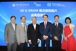
SAN JOSE, Calif., April 23, 2026 /PRNewswire/ -- NEO Semiconductor, a leading innovator in advanced AI and memory technologies, today announced successful proof-of-concept (POC) results for its 3D X-DRAM™ technology, marking a major milestone toward next-generation, high-density memory solutions for AI and data-centric systems.
The company also announced a new strategic investment led by Stan Shih, Founder and former Chairman and CEO of Acer, and former Board Director of TSMC for over 20 years. As a globally respected technology pioneer and entrepreneur, Mr. Shih's participation reflects strong confidence in NEO's technology and vision, and will support the company's next phase of development.
The POC test chips demonstrate that 3D X-DRAM can be manufactured using existing 3D NAND infrastructure, including established equipment, materials, and cost-efficient processes. With 3D NAND already exceeding 300 layers in production, these results pave the way for next-generation high-density 3D DRAM, while validating solid electrical performance and reliability.
Key POC results include:
- Read/write latency: <10 ns
- Data retention: >1 second at 85°C (15× better than the 64 ms JEDEC standard)
- Bit-line disturbance: >1 second at 85°C
- Word-line disturbance: >1 second at 85°C
- Endurance: >10¹⁴ cycles
"These results validate a new scaling path for DRAM," said Andy Hsu, Founder & CEO of NEO Semiconductor. "We believe this technology can enable significantly higher density, lower cost, and improved energy efficiency for the AI era. By leveraging established 3D NAND manufacturing processes and ecosystem, we aim to bring 3D DRAM to reality sooner. NEO is actively engaging with leading global memory and semiconductor companies on potential co-development opportunities, and we believe our technology is well suited for a scalable licensing and partnership model to bring next-generation AI memory solutions to market."
Industry analysts also highlighted the significance of the results. "At this pivotal moment, NEO Semiconductor has achieved a major breakthrough," said Jeongdong Choe, Senior Technical Fellow and SVP at TechInsights. "As conventional DRAM scaling approaches its limits, the industry is shifting toward 3D architectures and new cell technologies to meet growing AI and data-centric demands. NEO's silicon POC represents a significant milestone, demonstrating real-world viability beyond theoretical concepts. The reported electrical and reliability results are encouraging, and this development aligns with the industry roadmap toward vertically scaled memory. Much like the transition to 3D NAND over the past decade, we are now witnessing the dawn of a new 3D DRAM era beyond traditional scaling limits. It is truly exciting to see this vision becoming a tangible reality."
The POC was developed in collaboration with National Yang Ming Chiao Tung University (NYCU) in Taiwan, specifically its Industry-Academia Innovation School (IAIS), and was fabricated and tested at the National Institutes of Applied Research- Taiwan Semiconductor Research Institute (NIAR-TSRI). The device successfully passed extensive electrical and reliability evaluations, confirming the robustness and stability of the proposed memory architecture.
"I am pleased that this close industry–academia co-development partnership has validated the feasibility of NEO's 3D DRAM concept under real silicon process conditions," said Jack Sun, Senior Vice President of NYCU and Dean of IAIS, and former CTO of TSMC. "The successful proof-of-concept not only demonstrates the potential of innovative memory architectures, but also confirms the feasibility of implementing advanced memory technologies using mature processes. This collaboration among NEO, NYCU IAIS, and NIAR-TSRI further underscores the value of industry–academia partnerships in accelerating innovation from concept to practical implementation."
In parallel, NEO announced a strategic investment from a group of leading technology investors, led by Stan Shih, Founder and former Chairman and CEO of Acer. "I am delighted to see this breakthrough achieved through collaboration across industry and academia," said Stan Shih. "By bringing together innovation, strong engineering execution, and a robust semiconductor ecosystem in Taiwan, this POC was successfully realized. NEO's 3D DRAM is expected to play a key role in future system architectures. As next-generation memory becomes increasingly critical to AI computing, innovations like 3D X-DRAM have the potential to contribute significantly to the evolution of the global memory industry."
The funding has supported the successful development of the POC and will continue to advance the company's next phase, including array-level implementation, multi-layer test chip development, and deeper engagement with leading memory companies to explore strategic partnerships.
NEO is currently in active discussions with industry partners across the memory and semiconductor ecosystem to advance the technology toward commercialization. With successful POC validation and growing industry engagement, the company is entering a new phase focused on advancing 3D X-DRAM as a foundational technology for next-generation AI memory systems.
NEO Semiconductor's CEO, Andy Hsu, will deliver a keynote presentation at FMS: Future of Memory and Storage conference, where he will discuss the company's 3D X-DRAM™ technology and share deeper insights into the recently demonstrated proof-of-concept results, including key performance and reliability metrics. The event takes place August 4-6, 2026, at the Santa Clara Convention Center in California, USA. NEO Semiconductor will also be exhibiting at booth #507. To schedule a meeting at FMS 2026, please contact: [email protected].
About NEO Semiconductor
NEO Semiconductor is a high-tech company pioneering next-generation AI and memory technologies. Founded in 2012 and based in San Jose, California, the company focuses on redefining memory architecture to meet the growing demands of AI and data-centric computing. Its founder, Andy Hsu, holds a master's degree from Rensselaer Polytechnic Institute (RPI) and is the inventor of more than 120 granted patents.
NEO's key innovations include X-NAND™, 3D X-AI™, and X-HBM™, along with its flagship 3D X-DRAM™, a breakthrough architecture that leverages a 3D NAND-like structure to enable a scalable path toward high-density, energy-efficient memory. Following successful proof-of-concept validation, NEO is advancing this technology toward broader industry adoption, aiming to help shape the future of AI-driven memory systems.
Media and Analyst Contact:
Maya Lustig
Email: [email protected]
Photo - https://mma.prnewswire.com/media/2964231/NEO_Semiconductor.jpg
Photo - https://mma.prnewswire.com/media/2964136/3D_X_DRAM_POC.jpg
Logo - https://mma.prnewswire.com/media/2680564/NEO_Semiconductor_Logo.jpg
SOURCE NEO Semiconductor


Share this article