CEA-Leti to Implement Multiple EV Group Systems on Its New 300-mm Fab Line Dedicated to 3D Integration

ST. FLORIAN, Austria, April 19, 2011 /PRNewswire/ -- EV Group (EVG) today announced that its longtime customer and partner, industry-leading research center CEA-Leti (Grenoble, France), has installed multiple EVG tools in its industry-first 300-mm cleanroom dedicated to R&D and prototyping for 3D-integration applications. While Leti's new state-of-the-art facility is focused on R&D and prototyping, EVG's equipment will be leveraged with an eye toward widespread adoption of 3D technology for high-volume applications. Specifically, EVG's equipment will be used in 3D technology demonstrations for Leti's global customer base, as well as low-volume pilot production on 300-mm wafers with the end goal of transferring the processes to their industrial partners' high-volume manufacturing environments.
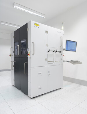
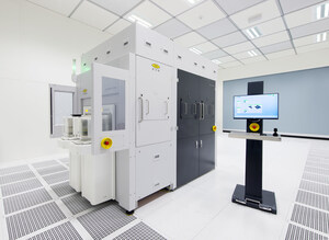
The EVG systems to be deployed on CEA-Leti's new 300-mm 3D line include an IQ Aligner production mask alignment system, a SmartView NT highest precision bond alignment system, an EVG560 production wafer bonding system and an EVG850 production bonding system for direct wafer bonding. These lithography and packaging systems were specifically chosen for the advantages they deliver in 3D-integration processing. Moreover, CEA-Leti will be able to tap EVG's extensive process know-how in 3D integration and through-silicon via (TSV) manufacturing, as the institute's 3D offerings include TSVs along with advanced capabilities in alignment, bonding, thinning and interconnects.
"These new tools offer important new capabilities to Leti and our partners," noted CEA-Leti CEO Laurent Malier. "Together we will demonstrate 3D and heterogeneous integration technologies on 300-mm wafers."
Paul Lindner, EV Group's executive technology director, said, "Our longstanding partnership with CEA-Leti has yielded significant advances for both companies as we have collaborated on new developments and leveraged each other's capabilities. By selecting our tools—including the industry's only production-proven 300-mm thermo compression wafer bonder—for its new facility, CEA-Leti is furthering its leading role in driving 3D technology advancement."
EVG works not only with research consortia and institutions such as CEA-Leti, but also with global consortia, including EMC-3D (which focuses on lowering the overall cost of 3D chips), SEMI, NILCOM (Consortium for Commercialization of Nanoimprint Lithography), NIL Austria, and Mancef (Micro and Nanotechnology Commercialization Education Foundation). Such initiatives are crucial in reducing the overall R&D costs of technology development, according to market-research firm Frost and Sullivan, which recently presented EVG with its 2010 Europe Product Innovation Award in Nanoimprint Technology. As a technology and market leader in lithography and nanoimprint lithography solutions, EVG is well positioned to continue driving and influencing the next generation of 3D-integration technology advancements.
About CEA-Leti
CEA is a French research and technology organisation, with activities in four main areas: energy, information technologies, healthcare technologies and defence and security. Within CEA, the Laboratory for Electronics & Information Technology (CEA-Leti) works with companies in order to increase their competitiveness through technological innovation and transfers. CEA-Leti is focused on micro and nanotechnologies and their applications, from wireless devices and systems, to biology and healthcare or photonics. Nanoelectronics and microsystems (MEMS) are at the core of its activities. As a major player in MINATEC campus, CEA-Leti operates 8,000-m2 state-of-the-art clean rooms, on 24/7 mode, on 200mm and 300mm wafer standards. With 1,700 employees, CEA-Leti trains more than 190 Ph.D. students and hosts 200 assignees from partner companies. Strongly committed to the creation of value for the industry, CEA-Leti puts a strong emphasis on intellectual property and owns more than 1,700 patent families. For more information, visit www.leti.fr.
About EV Group
EV Group (EVG) is a world leader in wafer-processing solutions for semiconductor, MEMS and nanotechnology applications. Through close collaboration with its global customers, the company implements its flexible manufacturing model to develop reliable, high-quality, low-cost-of-ownership systems that are easily integrated into customers' fab lines. Key products include wafer bonding, lithography/nanoimprint lithography (NIL) and metrology equipment, as well as photoresist coaters, cleaners and inspection systems.
In addition to its dominant share of the market for wafer bonders, EVG holds a leading position in NIL and lithography for advanced packaging and MEMS. Along these lines, the company co-founded the EMC-3D consortium in 2006 to create and help drive implementation of a cost-effective through-silicon via (TSV) process for major ICs and MEMS/sensors. Other target semiconductor-related markets include silicon-on-insulator (SOI), compound semiconductor and silicon-based power-device solutions.
Founded in 1980, EVG is headquartered in St. Florian, Austria, and operates via a global customer support network, with subsidiaries in Tempe, Ariz.; Albany, N.Y.; Yokohama and Fukuoka, Japan; Seoul, Korea and Chung-Li, Taiwan. The company's unique Triple i-approach (invent - innovate - implement) is supported by a vertical integration, allowing EVG to respond quickly to new technology developments, apply the technology to manufacturing challenges and expedite device manufacturing in high volume. More information is available at www.EVGroup.com.
SOURCE EV Group


Share this article